Backgrinding (Polishing/ BG Processing)
Mirror Polishing with Fine Mesh Grinding Wheels,
Improving Bending Strength and Thinning Wafers
We focus on finishing with fine mesh grinding wheels. Mirror polishing is also effective in improving bending strength. We have achieved stable wafers thinning to 40 μm (6 inch, 8 inch) and 100 μm for mass production by using a grinder.
We mainly handle backgrinding of semiconductor wafers, but we also accept requests for backgrinding and prototyping of individualized chips. Please feel free to contact us.
Wafer Backgrinding (BG)
The infeed method can stabilize the finishing thickness. In addition, we have a variety of grinding wheels for silicon wafers, and can grind according to your request. Ultra-thin finishing is possible, and we have a track record of 40 μm processing for 12 inches.
Fine Mesh Grinding Wheels
The grinding wheels are much finer than those of ordinary wheels. It is possible to process chips that are hard to break by reducing the crushed layer of the grinding wheels and increasing the bending strength. Furthermore, you can expect laser marks on the ground surface and improved bending strength.
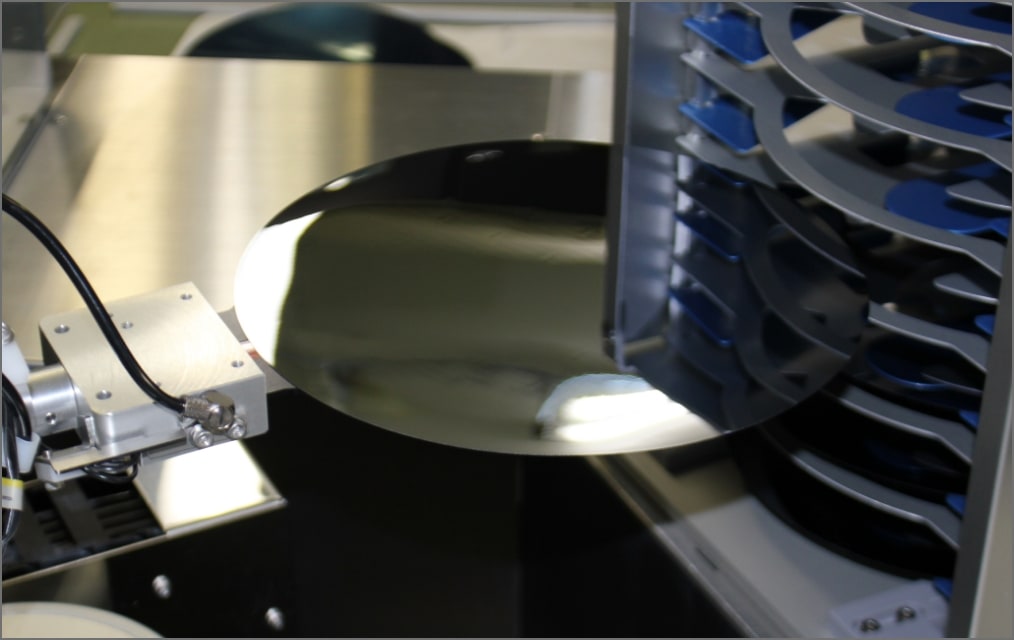
About Backgrinding
It is a process that thinly grinds materials such as silicon while pouring pure water on a rotating grinding wheels. The girinding wheels use diamond abrasive grains bonded with a bond.
Grinding is performed under optimal conditions for finishing thickness accuracy, finishing roughness, and flatness by adjusting the diamond abrasive grain size, bond material, rotation speed, descending speed, etc. In addition, it is possible to achieve a finish closer to a mirror surface by processing such as CMP and dry polishing.
In general, a finish with less roughness (closer to a mirror surface) is processed with higher bending strength (hardness to crack).
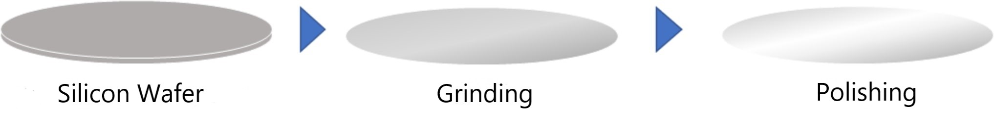
Wafer Polishing (Dry polishing, CMP)
The back surface of the wafer can be mirror-finished. (dry polishing/CMP) The fracture layer is reduced and the bending strength is increased, making it possible to process inserts that are hard to break. It also has the effect of reducing wafer warpage.
Equipment
| Equipment | Wafer Size | Number | Note |
|---|---|---|---|
| Protection Tape Attaching | Φ5 – 12 inch | 2 | |
| Grinders | Φ5 – 12 inch | 2 | Chip grinding possible |
| Dry Polishing | Φ6 – 12 inch | 2 | |
| CMP | Φ6 – 8 inch | 1 | |
| Protective Tape Removal | Φ5 – 12 inch | 1 | UV Radiation applied |
Specifications of Our Backside Grinding
-
Applications
·Silicon ・Compound Semiconductors (Partial)
-
Difficult to Process
·Ceramic ・Various Glasses
・Resin (Glass Epoxy, etc.) ·Metal -
Wafer Size
・Diameter 300mm or less
-
Wafer Thickness
・Base Thickness 1 mm or Less → Prototype 50 μm or More,
Mass production 100 μm or More -
Thickness Accuracy
・±2μm